- 您现在的位置:买卖IC网 > Sheet目录2004 > LTC1690IS8#TRPBF (Linear Technology)IC RCVR/DVR PAIR LOW PWR 8-SOIC
2
LTC1690
SYMBOL
PARAMETER
CONDITIONS
MIN
TYP
MAX
UNITS
VOD1
Differential Driver Output Voltage (Unloaded)
IO = 0
q
VCC
V
VOD2
Differential Driver Output Voltage (with Load)
R = 50
; (RS422)
q
2V
R = 22
or 27; (RS485), Figure 1
q
1.5
5
V
VOD3
Differential Driver Output Voltage (with Common Mode)
VTST = –7V to 12V, Figure 2
1.5
5
V
VOD
Change in Magnitude of Driver Differential Output
R = 22
, 27 or 50, Figure 1
q
0.2
V
Voltage for Complementary Output States
VTST = –7V to 12V, Figure 2
VOC
Driver Common Mode Output Voltage
R = 22
, 27 or 50, Figure 1
q
3V
|VOC|
Change in Magnitude of Driver Common Mode
R = 22
, 27 or 50, Figure 1
q
0.2
V
Output Voltage for Complementary Output States
VIH
Input High Voltage
Driver Input (D)
q
2V
VIL
Input Low Voltage
Driver Input (D)
q
0.8
V
IIN1
Input Current
Driver Input (D)
q
±2
A
IIN2
Input Current (A, B)
VCC = 0V or 5.25V, VIN = 12V
q
1mA
VCC = 0V or 5.25V, VIN = –7V
q
–0.8
mA
VTH
Differential Input Threshold Voltage for Receiver
–7V
≤ VCM ≤ 12V
q
– 0.20
– 0.01
V
VTH
Receiver Input Hysteresis
VCM = 0V
±30
mV
ABSOLUTE MAXIMUM RATINGS
W
WW
U
Supply Voltage (VCC) .............................................. 6.5V
Driver Input Voltage ..................... –0.3V to (VCC + 0.3V)
Driver Output Voltages ................................. –7V to 10V
Receiver Input Voltages .........................................
±14V
Receiver Output Voltage .............. –0.3V to (VCC + 0.3V)
Junction Temperature ........................................... 125
°C
Operating Temperature Range
LTC1690C ........................................ 0
°C ≤ TA ≤ 70°C
LTC1690I ..................................... – 40
°C ≤ TA ≤ 85°C
Storage Temperature Range ................. – 65
°C to 150°C
Lead Temperature (Soldering, 10 sec).................. 300
°C
(Note 1)
ORDER PART
NUMBER
MS8 PART MARKING
ORDER PART
NUMBER
LTC1690CMS8
LTDA
S8 PART MARKING
1690
1690I
LTC1690CN8
LTC1690IN8
LTC1690CS8
LTC1690IS8
Consult factory for Military Grade Parts
1
2
3
4
8
7
6
5
TOP VIEW
VCC
R
D
GND
A
B
Z
Y
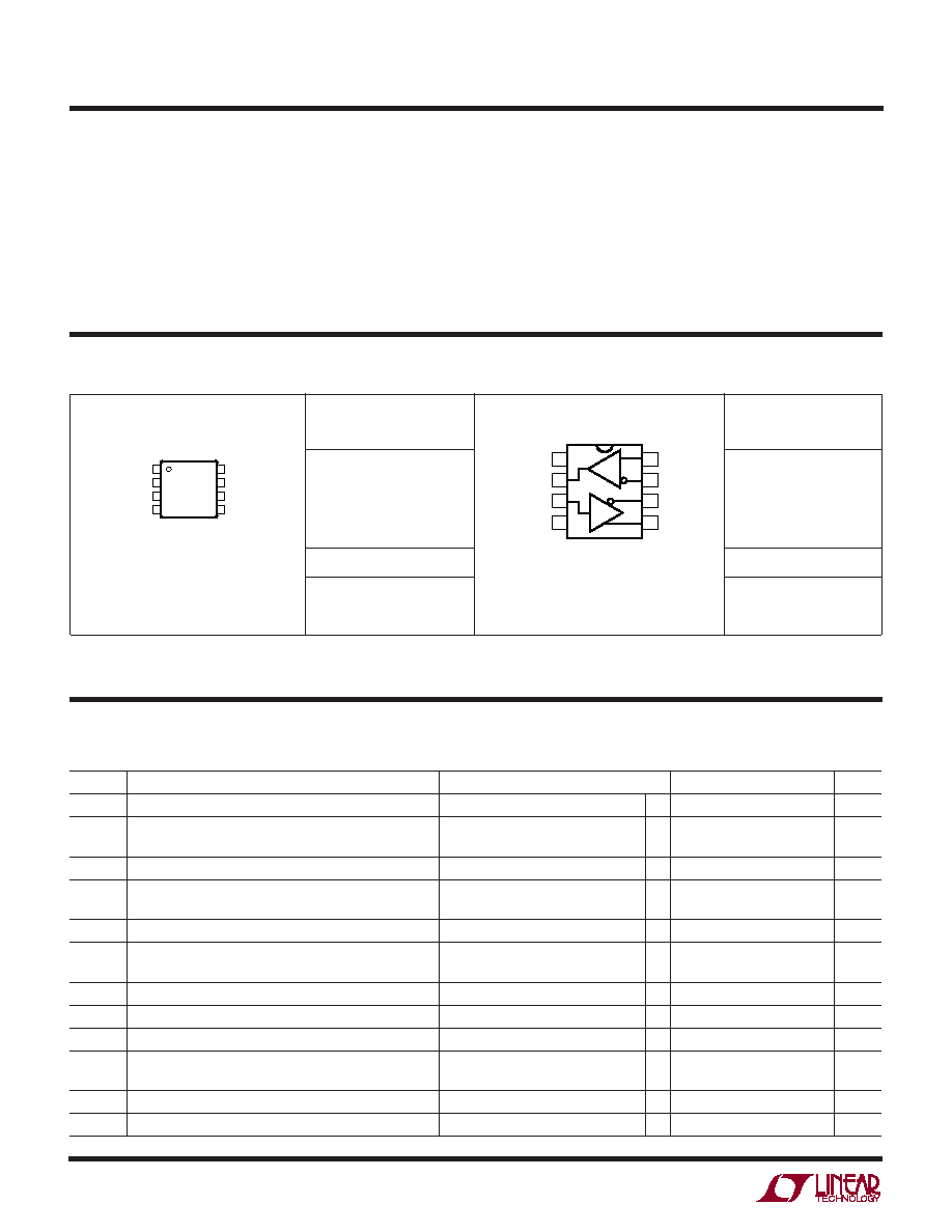
N8 PACKAGE
8-LEAD PLASTIC DIP
S8 PACKAGE
8-LEAD PLASTIC SO
D
R
TJMAX = 125°C, θJA = 130°C/W (N)
TJMAX = 125°C, θJA = 135°C/W (S)
1
2
3
4
8
7
6
5
TOP VIEW
MS8 PACKAGE
8-LEAD PLASTIC MSOP
VCC
R
D
GND
A
B
Z
Y
TJMAX = 125°C, θJA = 200°C/W
PACKAGE/ORDER INFORMATION
W
U
The q denotes the specifications which apply over the full operating
temperature range, otherwise specifications are at TA = 25°C. VCC = 5V ±5% (Notes 2, 3)
DC ELECTRICAL CHARACTERISTICS
发布紧急采购,3分钟左右您将得到回复。
相关PDF资料
LTC1740IG#TRPBF
IC ADC 14BIT 6MSPS 36SSOP
LTC1741IFW#PBF
IC ADC 12BIT 65MSPS 48-TSSOP
LTC1742CFW#TRPBF
IC ADC 14BIT 65MSPS 48-TSSOP
LTC1743IFW#PBF
IC ADC 12BIT 50MSPS SMPL 48TSSOP
LTC1744IFW#TRPBF
IC ADC 14BIT 50MSPS 48-TSSOP
LTC1745CFW#TRPBF
IC ADC 12BIT 25MSPS LN 48TSSOP
LTC1746IFW#TRPBF
IC ADC 14BIT 25MSPS LP 48TSSOP
LTC1747IFW#PBF
IC ADC 12BIT 80MSPS 48-TSSOP
相关代理商/技术参数
LTC1690IS8PBF
制造商:Linear Technology 功能描述:Differential Driver/Receiver Pair SOIC8
LTC1693-1CS8
功能描述:IC MOSFET DVR N-CH DUAL 8-SOIC RoHS:否 类别:集成电路 (IC) >> PMIC - MOSFET,电桥驱动器 - 外部开关 系列:- 标准包装:5 系列:- 配置:低端 输入类型:非反相 延迟时间:600ns 电流 - 峰:12A 配置数:1 输出数:1 高端电压 - 最大(自引导启动):- 电源电压:14.2 V ~ 15.8 V 工作温度:-20°C ~ 60°C 安装类型:通孔 封装/外壳:21-SIP 模块 供应商设备封装:模块 包装:散装 配用:BG2A-NF-ND - KIT DEV BOARD FOR IGBT 其它名称:835-1063
LTC1693-1CS8#PBF
功能描述:IC MOSFET DVR N-CH DUAL 8-SOIC RoHS:是 类别:集成电路 (IC) >> PMIC - MOSFET,电桥驱动器 - 外部开关 系列:- 标准包装:95 系列:- 配置:高端和低端,独立 输入类型:非反相 延迟时间:160ns 电流 - 峰:290mA 配置数:1 输出数:2 高端电压 - 最大(自引导启动):600V 电源电压:10 V ~ 20 V 工作温度:-40°C ~ 125°C 安装类型:表面贴装 封装/外壳:8-SOIC(0.154",3.90mm 宽) 供应商设备封装:8-SOIC 包装:管件 产品目录页面:1381 (CN2011-ZH PDF)
LTC1693-1CS8#TR
功能描述:IC DRVR MOSF DUAL N-CH HS 8SOIC RoHS:否 类别:集成电路 (IC) >> PMIC - MOSFET,电桥驱动器 - 外部开关 系列:- 标准包装:5 系列:- 配置:低端 输入类型:非反相 延迟时间:600ns 电流 - 峰:12A 配置数:1 输出数:1 高端电压 - 最大(自引导启动):- 电源电压:14.2 V ~ 15.8 V 工作温度:-20°C ~ 60°C 安装类型:通孔 封装/外壳:21-SIP 模块 供应商设备封装:模块 包装:散装 配用:BG2A-NF-ND - KIT DEV BOARD FOR IGBT 其它名称:835-1063
LTC1693-1CS8#TRPBF
功能描述:IC MOSFET DVR N-CH DUAL 8-SOIC RoHS:是 类别:集成电路 (IC) >> PMIC - MOSFET,电桥驱动器 - 外部开关 系列:- 标准包装:5 系列:- 配置:低端 输入类型:非反相 延迟时间:600ns 电流 - 峰:12A 配置数:1 输出数:1 高端电压 - 最大(自引导启动):- 电源电压:14.2 V ~ 15.8 V 工作温度:-20°C ~ 60°C 安装类型:通孔 封装/外壳:21-SIP 模块 供应商设备封装:模块 包装:散装 配用:BG2A-NF-ND - KIT DEV BOARD FOR IGBT 其它名称:835-1063
LTC1693-1IS8
功能描述:IC MOSFET DVR N-CH DUAL 8-SOIC RoHS:否 类别:集成电路 (IC) >> PMIC - MOSFET,电桥驱动器 - 外部开关 系列:- 标准包装:5 系列:- 配置:低端 输入类型:非反相 延迟时间:600ns 电流 - 峰:12A 配置数:1 输出数:1 高端电压 - 最大(自引导启动):- 电源电压:14.2 V ~ 15.8 V 工作温度:-20°C ~ 60°C 安装类型:通孔 封装/外壳:21-SIP 模块 供应商设备封装:模块 包装:散装 配用:BG2A-NF-ND - KIT DEV BOARD FOR IGBT 其它名称:835-1063
LTC1693-1IS8#PBF
功能描述:IC MOSFET DVR N-CH DUAL 8-SOIC RoHS:是 类别:集成电路 (IC) >> PMIC - MOSFET,电桥驱动器 - 外部开关 系列:- 标准包装:95 系列:- 配置:高端和低端,独立 输入类型:非反相 延迟时间:160ns 电流 - 峰:290mA 配置数:1 输出数:2 高端电压 - 最大(自引导启动):600V 电源电压:10 V ~ 20 V 工作温度:-40°C ~ 125°C 安装类型:表面贴装 封装/外壳:8-SOIC(0.154",3.90mm 宽) 供应商设备封装:8-SOIC 包装:管件 产品目录页面:1381 (CN2011-ZH PDF)
LTC1693-1IS8#TR
功能描述:IC DRVR MOSF DUAL N-CH HS 8SOIC RoHS:否 类别:集成电路 (IC) >> PMIC - MOSFET,电桥驱动器 - 外部开关 系列:- 标准包装:5 系列:- 配置:低端 输入类型:非反相 延迟时间:600ns 电流 - 峰:12A 配置数:1 输出数:1 高端电压 - 最大(自引导启动):- 电源电压:14.2 V ~ 15.8 V 工作温度:-20°C ~ 60°C 安装类型:通孔 封装/外壳:21-SIP 模块 供应商设备封装:模块 包装:散装 配用:BG2A-NF-ND - KIT DEV BOARD FOR IGBT 其它名称:835-1063